(China (Mainland))

Product Summary
The Virtex-5 family provides the newest most powerful features in the FPGA market. Using the second generation ASMBl (Advanced
Silicon Modular Block) column-based architecture, the Virtex-5 family contains five distinct platforms (sub-families), the most choice
offered by any FPGA family. Each platform contains a different ratio of features to address the needs of a wide variety of advanced logic
designs. In addition to the most advanced, high-performance logic fabric, Virtex-5 FPGAs contain many hard-IP system level blocks,
including powerful 36-Kbit block RAM/FIFOs, second generation 25 x 18 DSP slices, SelectIO technology with built-in digitallycontrolled impedance, ChipSync source-synchronous interface blocks, system monitor functionality, enhanced clock management tiles
with integrated DCM (Digital Clock Managers) and phase-locked-loop (PLL) clock generators, and advanced configuration options.
Additional platform dependant features include power-optimized high-speed serial transceiver blocks for enhanced serial connectivity,
PCI Express compliant integrated Endpoint blocks, tri-mode Ethernet MACs (Media Access Controllers), and high-performance
PowerPC 440 microprocessor embedded blocks.
Features
(1) Five platforms LX, LXT, SXT, TXT, and FXT;
(2) Virtex-5 LX: High-performance general logic applications;
(3) Virtex-5 LXT: High-performance logic with advanced serial connectivity;
(4) Virtex-5 SXT: High-performance signal processing applications with advanced serial connectivity;
(5) Virtex-5 TXT: High-performance systems with double density advanced serial connectivity;
(6) Virtex-5 FXT: High-performance embedded systems with advanced serial connectivity;
(7) Cross-platform compatibility;
(8) LXT, SXT, and FXT devices are footprint compatible in the same package using adjustable voltage regulators;
(9) Most advanced, high-performance, optimal-utilization,FPGA fabric;
(10) Real 6-input look-up table (LUT) technology;
(11) Dual 5-LUT option; (18)? Improved reduced-hop routing; (12) 64-bit distributed RAM option;
(13) SRL32/Dual SRL16 option;
(14) Powerful clock management tile (CMT) clocking;
(15) Digital Clock Manager (DCM) blocks for zero delay buffering, frequency synthesis, and clock phase shifting;
(16) PLL blocks for input jitter filtering, zero delay buffering,frequency synthesis, and phase-matched clock division;
(17) 36-Kbit block RAM/FIFOs;
(19) True dual-port RAM blocks;
(20) Enhanced optional programmable FIFO logic;
(21) Programmable- True dual-port widths up to x36- Simple dual-port widths up to x72;
(22) Built-in optional error-correction circuitry;
(23) Optionally program each block as two independent 18-Kbit ; blocks;
(24) High-performance parallel SelectIO technology;
(25) 1.2 to 3.3V I/O Operation;
(26) Source-synchronous interfacing using ChipSync?technology;
(27) Digitally-controlled impedance (DCI) active termination;
(28) Flexible fine-grained I/O banking;
(29) High-speed memory interface support;
| Image | Part No | Mfg | Description |  |
Pricing (USD) |
Quantity | ||||||
|---|---|---|---|---|---|---|---|---|---|---|---|---|
 |
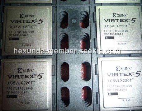
 XC5VLX220T-1FFG1738C |
|
IC FPGA VIRTEX-5 220K 1738FBGA |
Data Sheet |
|
|
||||||
| Image | Part No | Mfg | Description | |
Pricing (USD) |
Quantity | ||||||
 |
XC5VFX100T-1FF1136I |
|
IC FPGA VIRTEX-5FXT 1136FFBGA |
Data Sheet |
|
|
||||||
|
XC5VFX100T-1FF1738I |
|
IC FPGA VIRTEX-5FXT 1738FFBGA |
Data Sheet |
|
|
||||||
|
XC5VFX100T-1FFG1136C |
|
IC FPGA VIRTEX 5 100K 1136FFGBGA |
Data Sheet |
|
|
||||||
|
XC5VFX100T-1FFG1136I |
|
IC FPGA VIRTEX 5 100K 1136FFGBGA |
Data Sheet |
|
|
||||||
|
XC5VFX100T-1FFG1738C |
|
IC FPGA VIRTEX 5 100K 1738FFGBGA |
Data Sheet |
|
|
||||||
|
XC5VFX100T-1FFG1738I |
|
IC FPGA VIRTEX 5 100K 1738FFGBGA |
Data Sheet |
|
|
||||||