(China (Mainland))

Product Summary
The AD8362 is a true rms-responding power detector that has a 65 dB measurement range. It is intended for use in a variety of high frequency communication systems and in instrumentation requiring an accurate response to signal power. It is easy to use, requiring only a single supply of 5 V and a few capacitors. It can operate from arbitrarily low frequencies to over 3.8 GHz and can accept inputs that have rms values from 1 mV to at least 1 V rms, with large crest factors, exceeding the requirements for accurate measurement of CDMA signals. The input signal is applied to a resistive ladder attenuator that comprises the input stage of a variable gain amplifier (VGA). The 12 tap points are smoothly interpolated using a proprietary technique to provide a continuously variable attenuator, which is controlled by a voltage applied to the VSET pin. The resulting signal is applied to a high performance broadband amplifier. Its output is measured by an accurate square-law detector cell. The fluctuating output is then filtered and compared with the output of an identical squarer, whose input is a fixed dc voltage applied to the VTGT pin, usually the accurate reference of 1.25 V provided at the VREF pin.
The difference in the outputs of these squaring cells is integrated in a high gain error amplifier, generating a voltage at the VOUT pin with rail-to-rail capabilities. In a controller mode, this low noise output can be used to vary the gain of a host system RF amplifier, thus balancing the setpoint against the input power. Optionally, the voltage at VSET can be a replica of the RF signal amplitude modulation, in which case the overall effect is to remove the modulation component prior to detection and lowpass filtering. The corner frequency of the averaging filter can be lowered without limit by adding an external capacitor at the CLPF pin. The AD8362 can be used to determine the true power of a high frequency signal having a complex low frequency modulation envelope, or simply as a low frequency rms voltmeter. The high-pass corner generated by its offset-nulling loop can be lowered by a capacitor added on the CHPF pin. Used as a power measurement device, VOUT is strapped to VSET. The output is then proportional to the logarithm of the rms value of the input. In other words, the reading is presented
directly in decibels and is conveniently scaled 1 V per decade, or 50 mV/dB; other slopes are easily arranged. In controller modes, the voltage applied to VSET determines the power level required at the input to null the deviation from the setpoint. The output buffer can provide high load currents. The AD8362 has 1.3 mW power consumption when powered down by a logic high applied to the PWDN pin. It powers up within about 20s to its nominal operating current of 20 mA at 25C. The AD8362 is supplied in a 16-lead TSSOP for operation over the temperature range of 0C to +85C.
Features
(1)Complete fully calibrated measurement/control system ;
(2)Accurate rms-to-dc conversion from 50 Hz to 3.8 GHz ;
(3)Input dynamic range of >65 dB: ?52 dBm to +8 dBm in 50 鎯?; (4)Waveform and modulation independent, such as ;
(5)GSM/CDMA/TDMA ;
(6)Linear-in-decibels output, scaled 50 mV/dB ;
(7)Law conformance error of 0.5 dB ;
(8)All functions temperature and supply stable ;
(9)Operates from 4.5 V to 5.5 V at 24 mA ;
(10)Power-down capability to 1.3 mW
| Image | Part No | Mfg | Description |  |
Pricing (USD) |
Quantity | ||||||||||||||||
|---|---|---|---|---|---|---|---|---|---|---|---|---|---|---|---|---|---|---|---|---|---|---|
 |
 AD8362ARUZ |
|
IC PWR DETECTOR 3.8GHZ 16-TSSOP |
Data Sheet |
|
|
||||||||||||||||
|
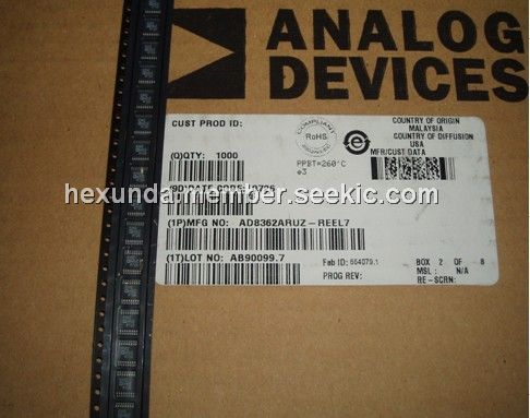
AD8362ARUZ-REEL7 |
|
IC PWR DETECTOR 3.8GHZ 16-TSSOP |
Data Sheet |
|
|
||||||||||||||||
 |
AD8362ARUZ-REEL71 |
Other |
|
Data Sheet |
Negotiable |
|
||||||||||||||||